Asic Services

Key ASIC's professional ASIC Design / Production (OEM) approach and flexible engagement model provide customers with confidence, control and ownership over the whole development process. Our customers may contract Key ASIC's Turnkey Services in whole or in part, without restrictions on business or volume size. Key ASIC's objective is to meet customers' chip design needs, accelerate their development process and deliver market proven silicon products in the shortest time and the lowest cost.

Key ASIC's ASIC Design Flow & Engagement Models

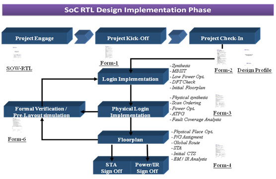
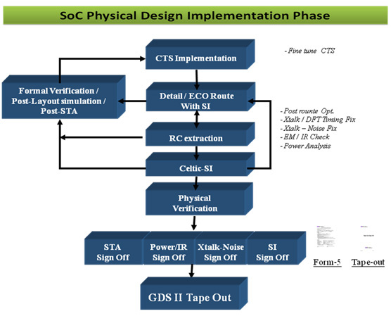
Asic Services Design Flow

To help customers successfully implement their chip from specification to delivery of physical silicon, Key ASIC offers efficient, reliable and complete design methodology and tools. Key ASIC's design methodology applies leading edge commercial EDA tools, as well as proprietary utilities to form a streamlined process for today's ASIC design.

Key ASIC's state-of-the-art design methodology includes all aspects required for advancing chip design:

Feasibility analysis, timing closure, power-integrity, signal-integrity, reliability, complexity, testability, design for manufacturability, and high density substrate design.


Asic Services Package and Test

As design complexity increases, packaging and testing represent a significant portion of the overall chip cost. Key ASIC works closely with industry partners to provide a wide selection of advanced and cost effective package & test offerings, such as high-speed interface, low power dissipation greater choice and flexibility translate to minimum cost for our customers.

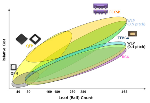
Package Options
Partnering with leading packaging vendors like ASE, OSE, Key ASIC provides a wide range of package solutions from complex System-in-Package (SiP), Ball-Grid-Array (BGA) to the cost-sensitive Quad Flat Pack (QFP) in order to satisfy customers' increasing demands for smaller sizes, more I/Os, and lower costs.


Testing Program and Test Environment
The test program and environment prepared for each ASIC prototype are developed and monitored carefully by a group of experienced in-house engineers.

At the mass production stage when all of the settings of a test program are confirmed, the test program and the production documents are sent to our test partners to ensure accuracy before production begins. Only after careful verification will the test program be formally released to our test partner. Various tester choices are supported for different performance/cost requirements through qualified outside partners who meet customers' capacity and cost objectives.

Asic Services Process

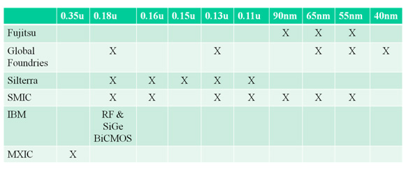
Key ASIC offers both fabless chip design companies and system houses the commercial benefits of an IC foundry production approach without the cost of ownership or volume requirements associated with a seamless supply chain. Key ASIC provides access to the leading foundries all over the world including Silterra, SMIC, Globalfoundries, Fujitsu, MXIC and IBM. This access provides a vast choice of silicon technologies covering a wide range of design requirements. Process ranges from 0.25um down to 40nm, crossing CMOS and specialty technologies are supported.

In addition to comprehensive foundry partners, Key ASIC possesses high level domain knowledge including:
– Touch panel drivers & controllers
– Storage devices
– Audio processors
– WiFi Secure Digitals
– ARM SOC

Process technologies available from Key ASIC are:

To learn shuttle schedule of each technology node, please contact us here.

Asic Services Production

Key ASIC is fully committed to providing our customers with unparalleled manufacturing flexibility, optimal value, quickest time-to-market silicon solutions and a dedication to customer service with our unique one-stop production management expertise.

Key ASIC's Unique One-Stop Production Management Package